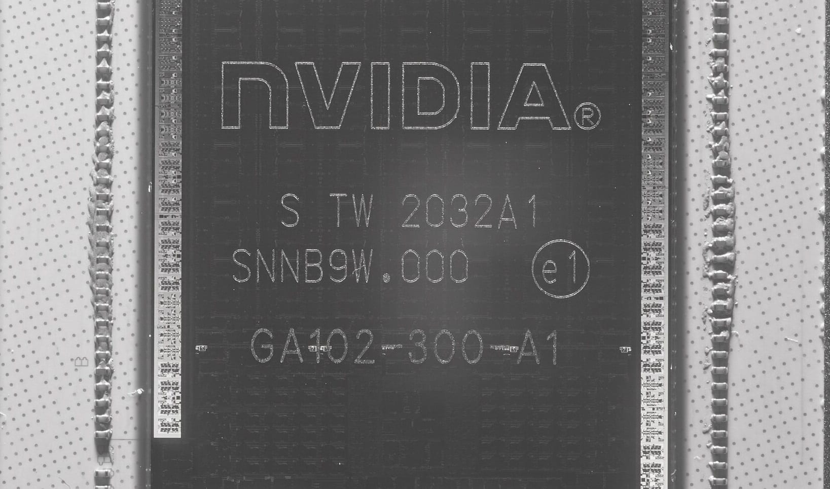
The first detailed images of the GA102 crystal appeared on the network. It gave life to two top-end NVIDIA graphics adapters of the Ampere generation: GeForce RTX 3090 and RTX 3080. Just like in the case of summer photos of Zen 3 crystals, our old friend Fritzchens Fritz shared photos of the GA102 matrix.
In order to get such detailed high-resolution photos, the enthusiast used special equipment. The results of Fritz’s work turned out to be very curious:
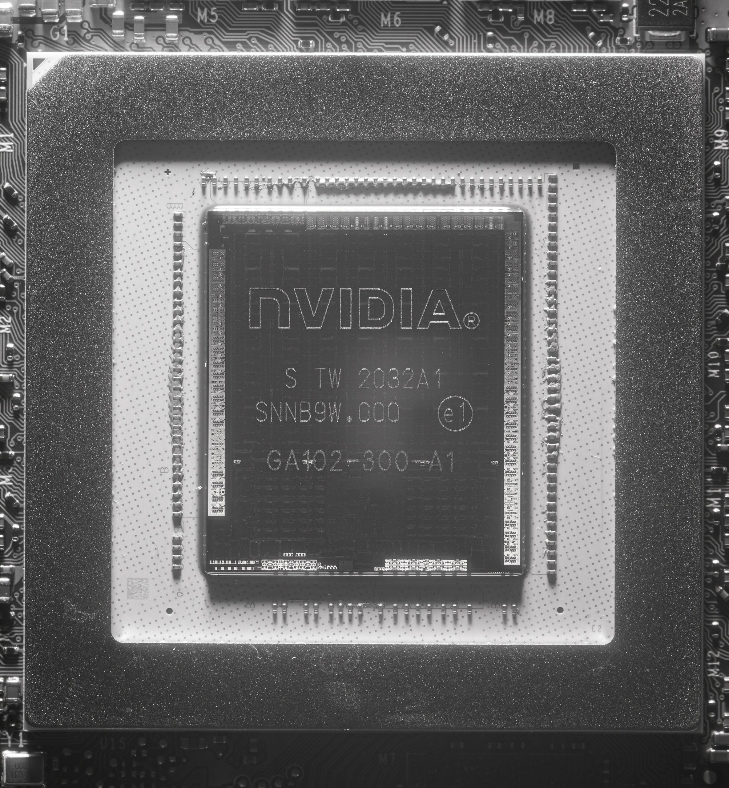
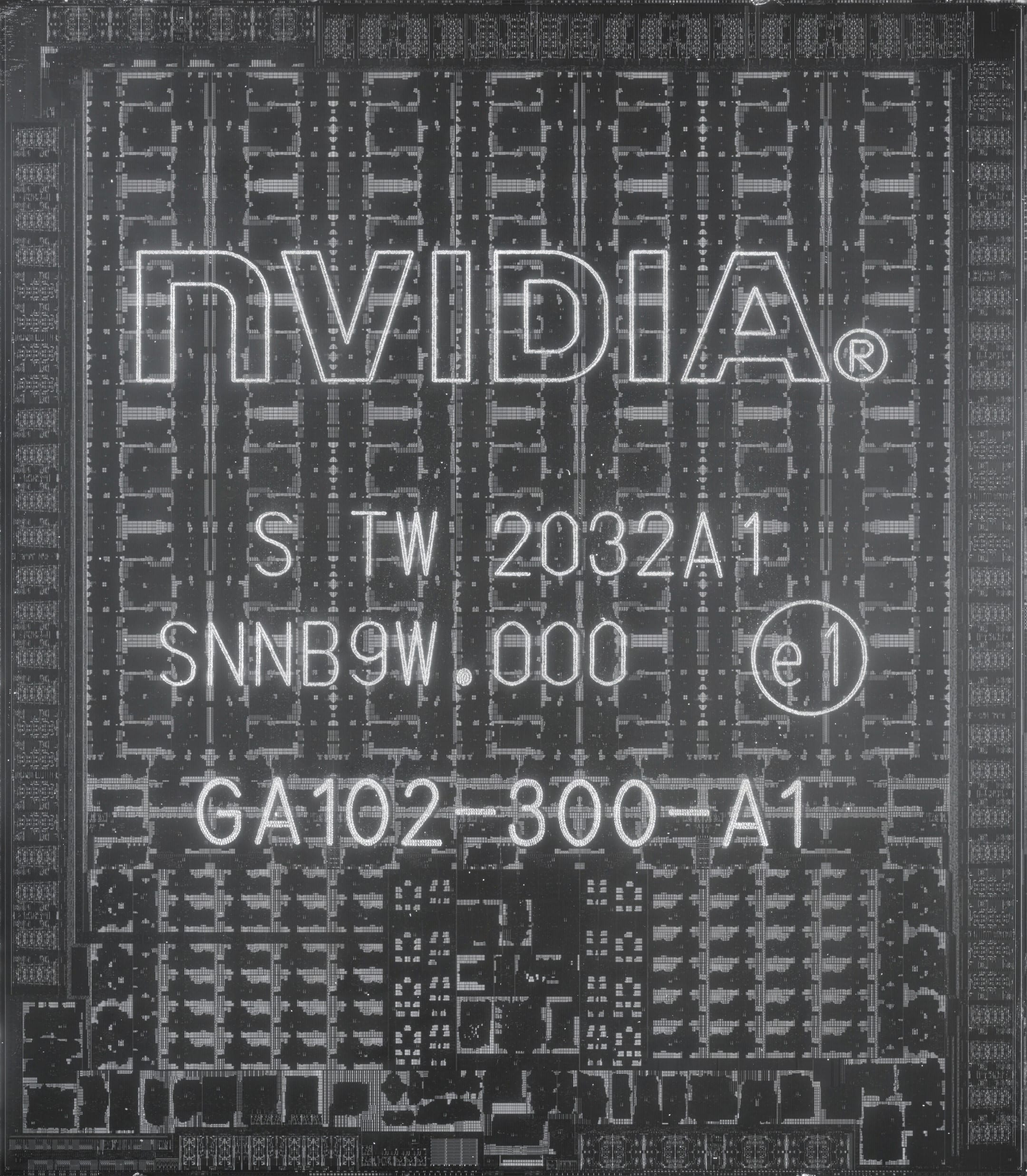
The NVIDIA GA102 Ampere chip consists of 28.3 billion transistors and has 10,752 active CUDA cores. The cache memory takes up quite a lot of space: the top GPU has 10 MB of L1 cache and 6 MB of L2 cache. Crystal size 628.4 mm2.
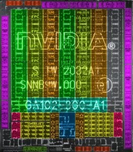
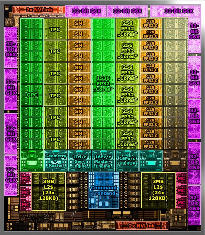
In fact, ~ 25% of the GPU area is occupied by INT32 and FP32 units, and about the same number of ROP (rasterization units), TMU (texture units), and SP (shader processors). Along the perimeter of the main execution units, there are twelve 32-bit GDDR6X video memory controllers (which ultimately give a 384-bit memory bus) and 4 NVLinks.
For more information on the GA102 matrix, head over to Locuza’s Twitter. The enthusiast talks in some detail about the structure of various crystals from AMD, Intel, and NVIDIA.