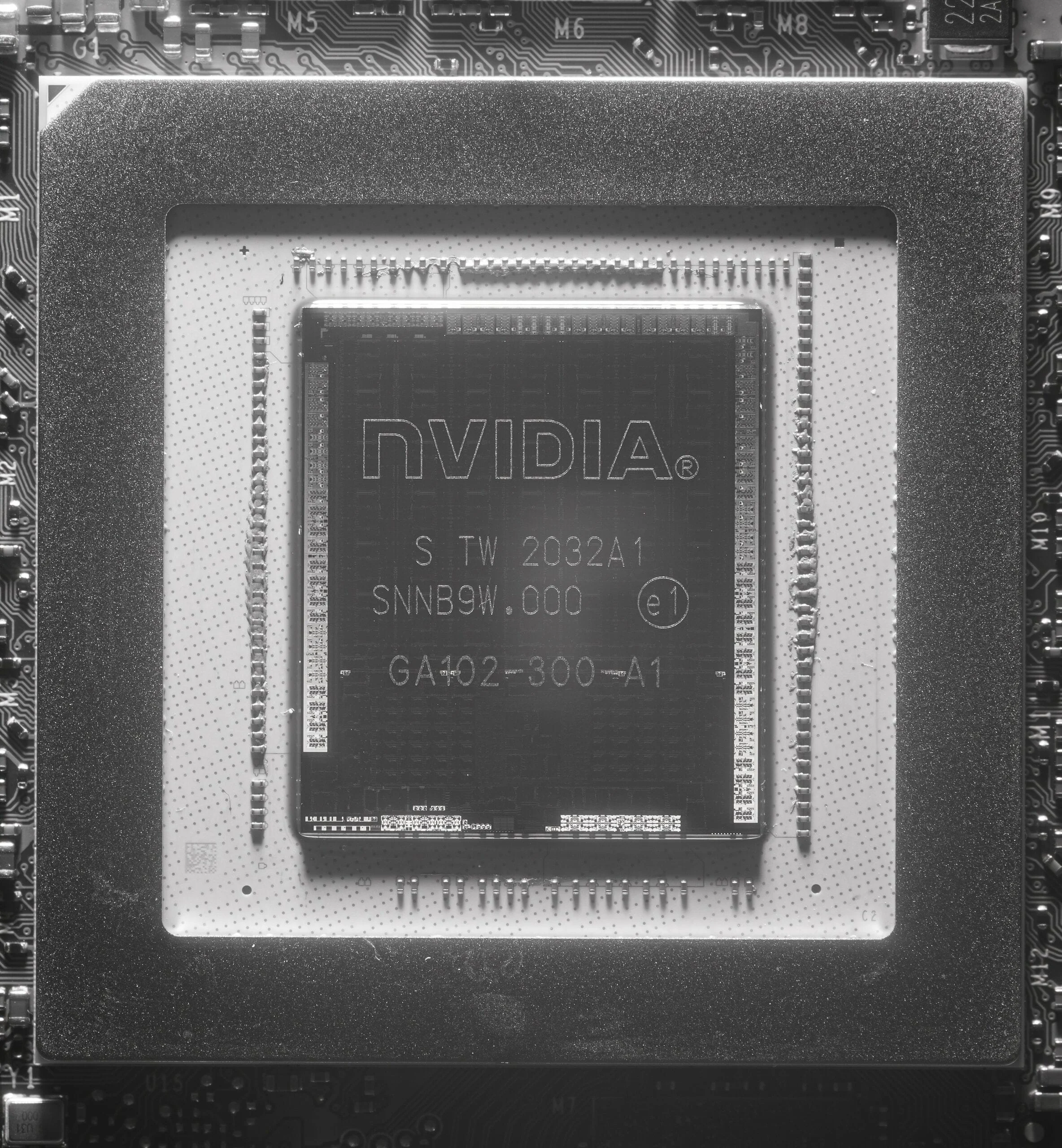
![A closer look at GA102 die shots [RTX 3090 and RTX 3080 graphics cards]](https://umtale-media.s3.eu-central-1.amazonaws.com/images/content/1e0457e3-2898-4285-9402-a1acc4aacc95.webp)
NEWS · HARDWARE
PUBLISHED
READING1 min
A closer look at GA102 die shots [RTX 3090 and RTX 3080 graphics cards]
The first detailed die shots of the GA102 GPU, which powers NVIDIA's flagship GeForce RTX 3090 and RTX 3080 graphics cards, have surfaced online.
The first detailed die shots of the GA102 silicon, which powers NVIDIA's flagship Ampere graphics cards, the GeForce RTX 3090 and RTX 3080, have surfaced online. Just like with the Zen 3 die shots from last summer, these GA102 photos were shared by our old friend Fritzchens Fritz.
X (Twitter)
By loading, you allow content from X (Twitter) (cookies may be set).
To capture these high-resolution close-ups, the enthusiast used specialized equipment. Fritz's results are highly intriguing:
 ⤢ ВІДКРИТИ
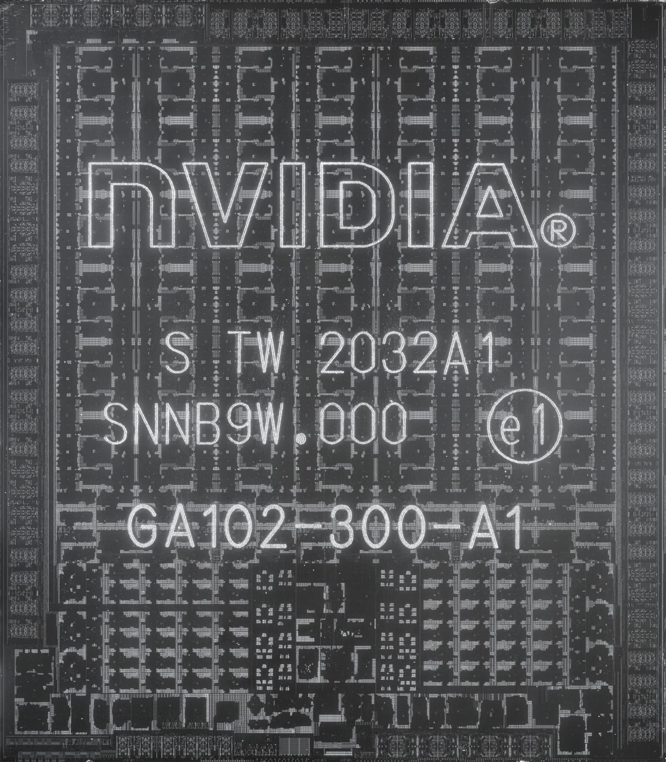 ⤢ ВІДКРИТИ
NVIDIA's GA102 Ampere chip packs 28.3 billion transistors and features 10,752 active CUDA cores. Cache memory takes up a significant portion of the die, with the flagship GPU packing 10 MB of L1 cache and 6 MB of L2 cache. The die size measures 628.4 mm².
X (Twitter)
By loading, you allow content from X (Twitter) (cookies may be set).
In fact, INT32 and FP32 blocks take up about 25% of the GPU's area, with roughly the same amount dedicated to ROPs, TMUs, and shader processors. Twelve 32-bit GDDR6X memory controllers surround the main execution blocks, enabling a 384-bit memory bus, alongside four NVLink interfaces.
If you want a deeper dive into the GA102 silicon, head over to Locuza's Twitter feed. The enthusiast regularly posts detailed breakdowns of various AMD, Intel, and NVIDIA dies.