BLOGS · OVERCLOCKING
PUBLISHED
READING7 min
Retro overclocking: pushing the Intel Core 2 Duo E6300 to the limit
Dive into the overclocking potential of the vintage dual-core Intel Core 2 Duo E6300 (L2 revision, Conroe 2M) with a quick round of benchmarks and games.
Back in 2012, we already explored the overclocking potential of the Intel Core 2 Duo E6300 processor, and frankly, repeating that test wouldn't make much sense. However, there's always a catch: an E6300 sample with the L2 stepping landed in our lab.
Quick history lesson, if you're interested. As far as I know, the E6300 was produced in only two revisions: B2, which was essentially a Conroe 4M (143 mm² die area) with half of its L2 cache disabled, and L2, which was a true Conroe 2M (111 mm² die area) with a physically two-megabyte cache. What do we know about the full-fledged Conroe 4M? That's right—its FSB wall is much higher than its smaller sibling, the Conroe 2M. Thus, from a purely technical (or even physical) standpoint, B2 and L2 are literally different dies, even though they're based on the same Core architecture. Therefore, exploring the overclocking potential of the "smaller" E6300 should be quite interesting. Right? Right?...
Processor
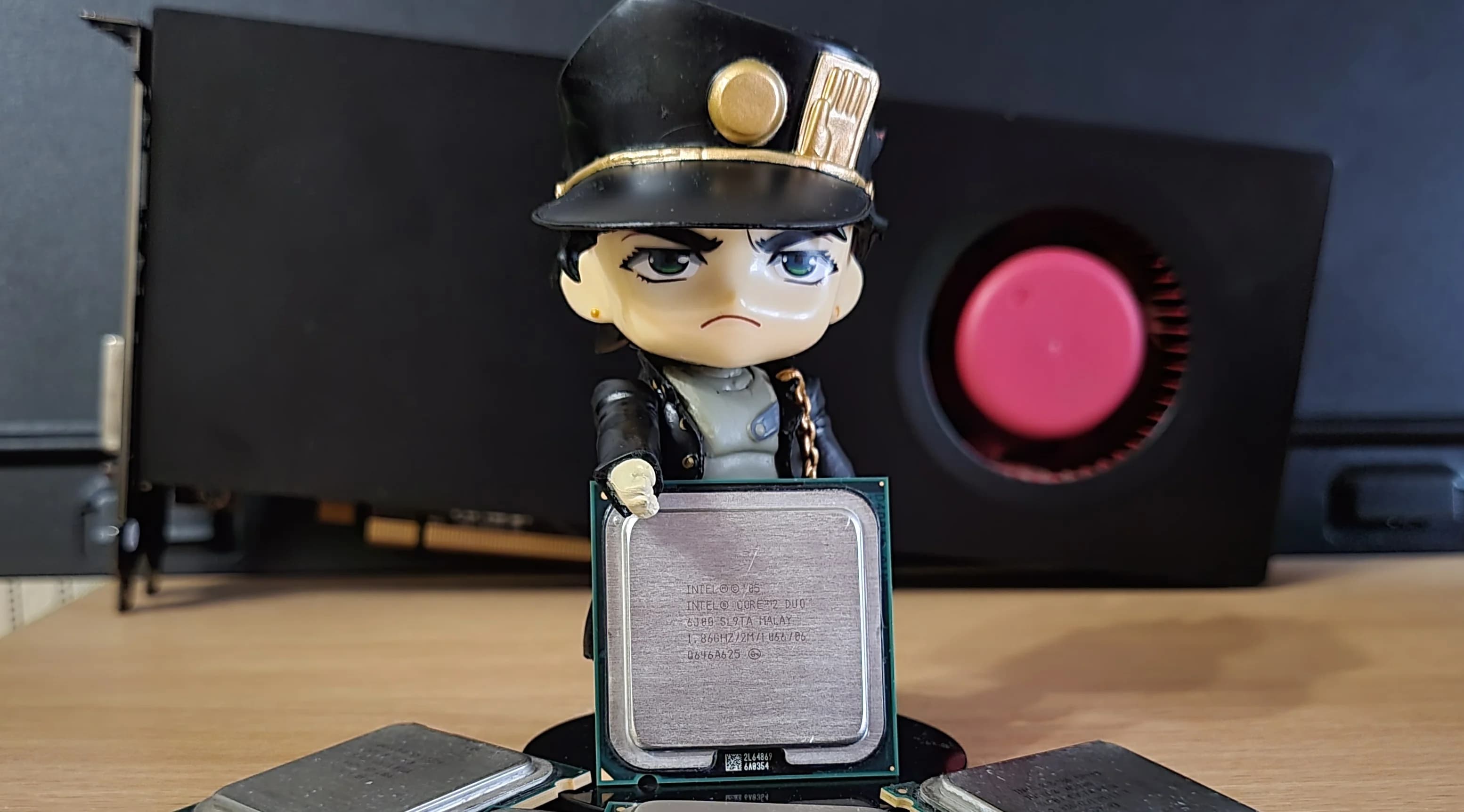
The test sample's marking is SL9TA. The chip was manufactured in Malaysia in 2006.
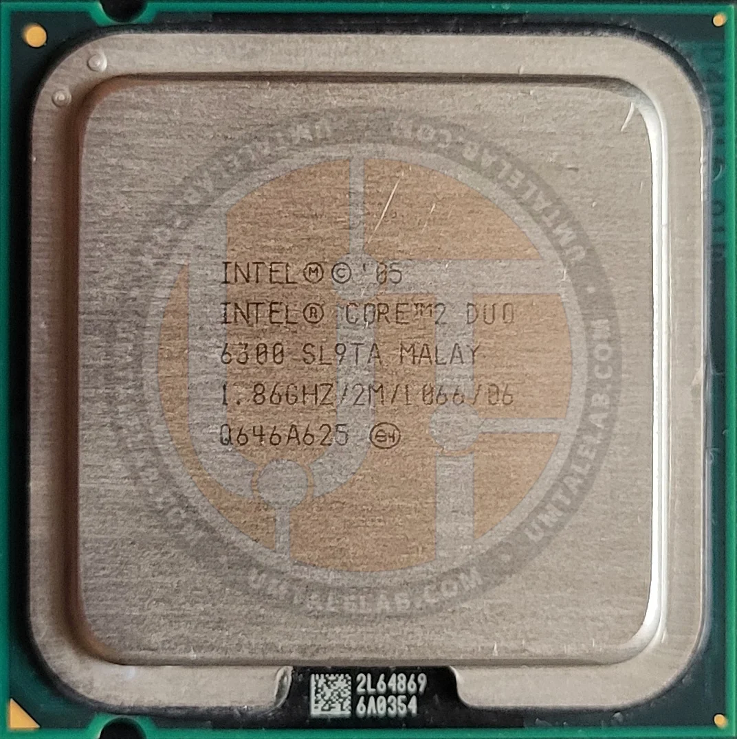
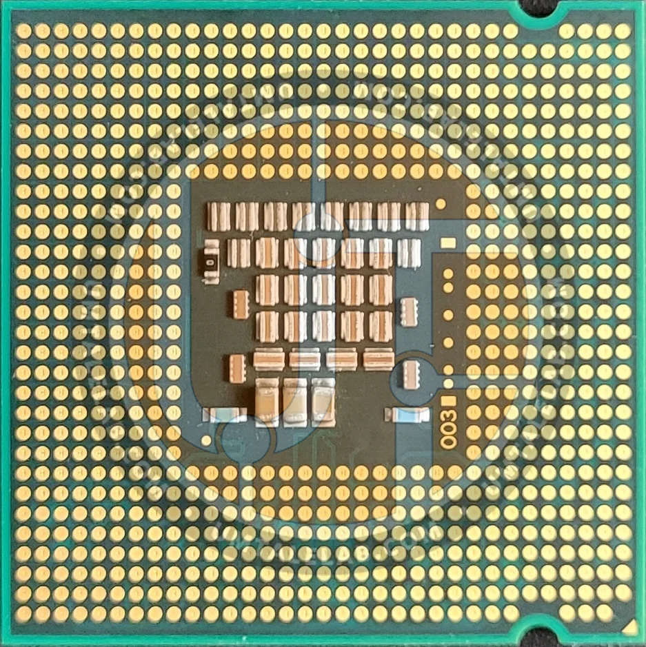
The Core 2 Duo E6300's codename is Conroe (Core architecture). Beneath this CPU's integrated heat spreader (IHS) lies a single 65nm dual-core monolithic die in the 2M modification.
As I mentioned earlier, our test sample's revision is L2, and this is the main difference from the 2012 article.
 ⤢ ВІДКРИТИ
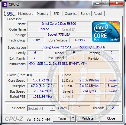
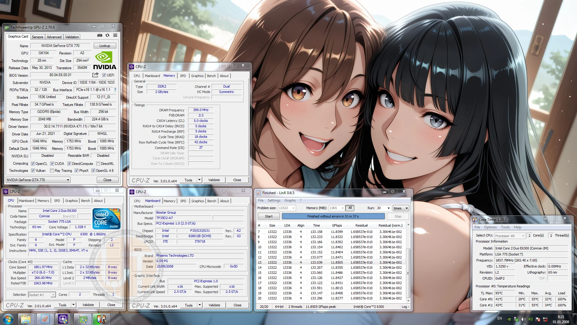
The Core 2 Duo E6300 features two cores with a nominal frequency of 1866 MHz (a 7x multiplier, 266 MHz bus frequency, and an effective frequency of 1066 MHz for core communication with the chipset and memory controller). The chip has 2048 KB of L2 cache, a default CPU voltage set at 1.344 volts, and an E6300 TDP that shouldn't exceed 65 watts.
The motherboard chipset handles RAM support for the test processor, as the E6300 itself doesn't have an integrated memory controller on its die. In our case, this means DDR2, but if you have a more modern board, such as one with a P45 or X48 chipset, it might feature DDR3 slots.
Test Rig
 ⤢ ВІДКРИТИ
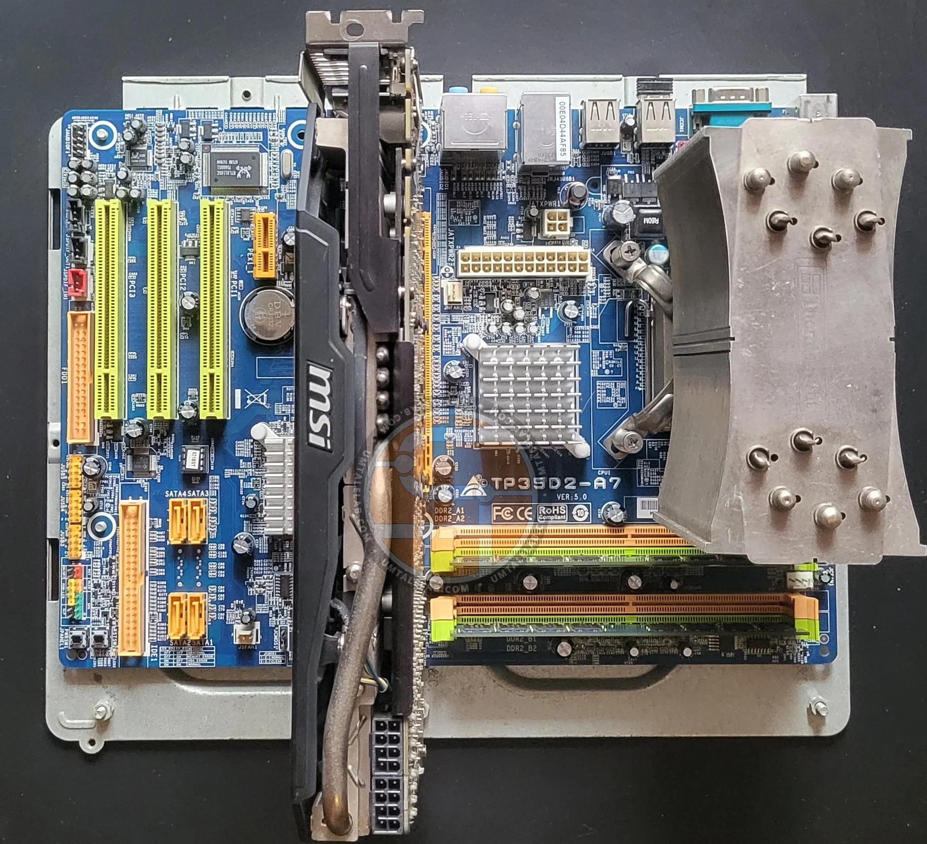
Processor — Core 2 Duo E6300;
Cooler — Thermalright Ultra-120 eXtreme;
RAM — 2x 1GB Nanya Technology modules, for a total of 2GB;
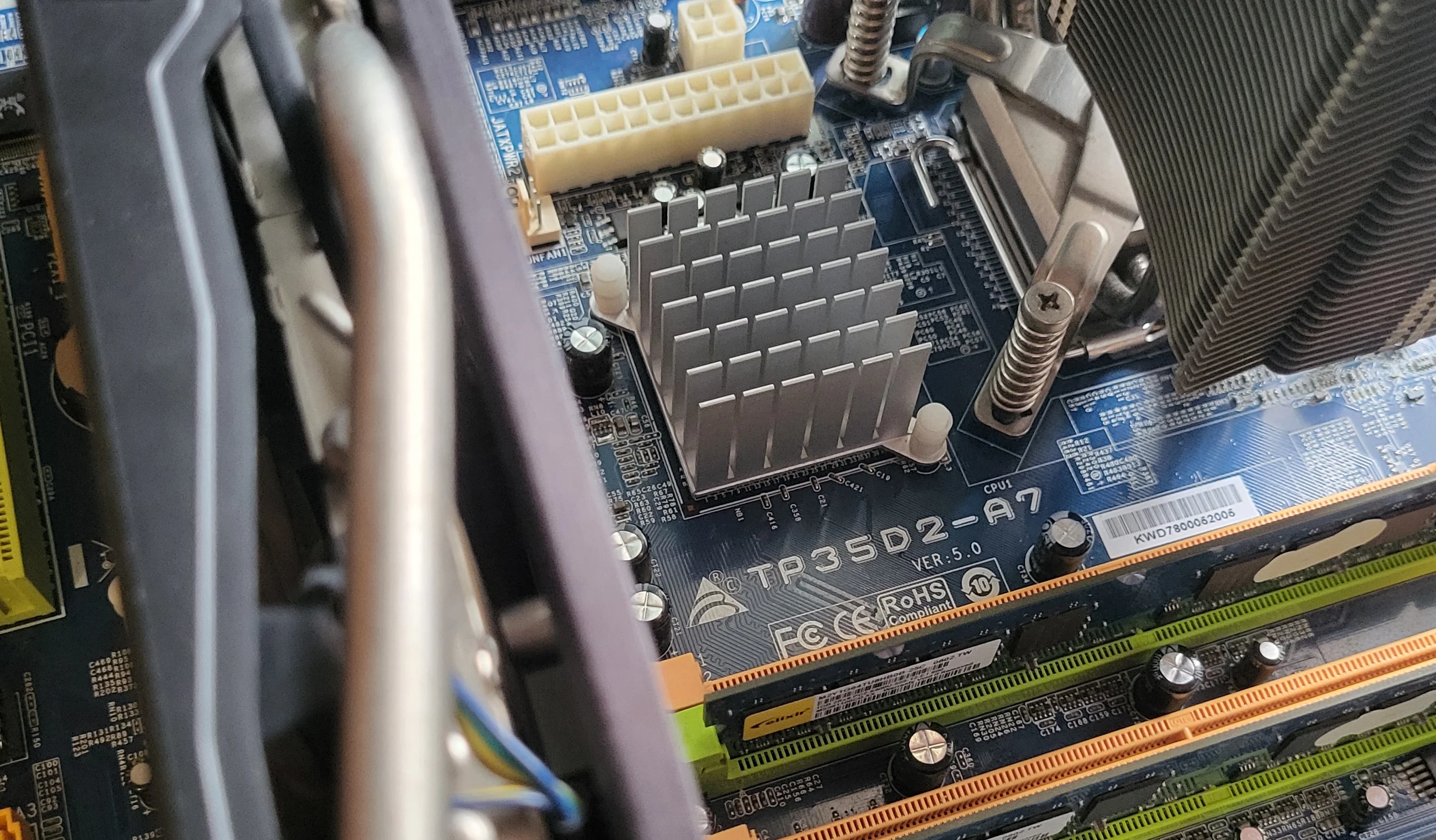
Motherboard — Biostar TP35D2-A7;
Graphics card — MSI GTX 770 Gaming OC 2GB (~1085/7000 MHz, Power Limit 115%);
SSD — KINGSTON 120GB SA400S37120G (Windows 7/Apps);
Hard drive — Seagate 2TB ST2000DM008-2FR102 (Games);
Power supply — Chieftec GPS-1250C.
 ⤢ ВІДКРИТИ
Core 2 Duo E6300 Overclocking
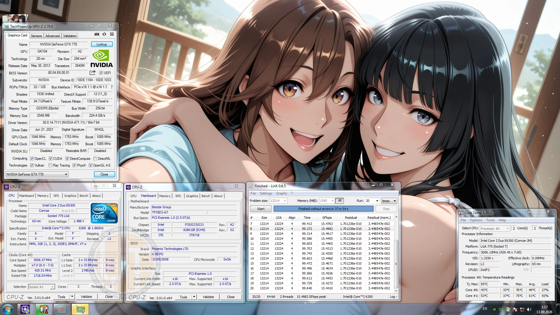
At the stock core voltage of 1.344 volts, the test sample only reached 2733 MHz, which is an incredibly poor result, even for an L2 stepping E6300. Increasing the voltage to 1.4 volts slightly pushed the frequency ceiling to 2844 MHz, while 1.42 volts allowed it to reach 2933 MHz. The chip only managed to break the 3 GHz barrier at 1.48 volts.
 ⤢ ВІДКРИТИ
And that was it. Literally. We hit the FSB wall. The motherboard simply refused to boot if the FSB was raised even 1 MHz above 430, without any blue screens, errors, or other "signs." I tried "playing" with the VTT FSB and chipset voltages, but it yielded no positive results.
Core 2 Duo E6300 overclocking settings to 3006 MHz in BIOS
Core voltage — 1.48 volts (+0.136 over nominal, multimeter showed a physical 1.456 volts);
Bus frequency — 429 MHz;
Bus multiplier - 7;
Bus voltage — 1.250 volts (+0.00 over nominal - stock);
RAM multiplier in BIOS — 400 MHz (with overclocking, the effective memory frequency was 858 MHz);
RAM voltage — 2.100 volts (+0.200 over nominal).
For example, the B2 stepping E6300 we tested back in 2012 easily hit 3360 MHz at 1.424 volts before also hitting a "wall".
This illustrates the difference between two revisions of the same processor. If you're looking for a high-quality E6300 chip for extreme overclocking, carefully check its markings. This will help you avoid accidentally picking up an L2 revision.
Quick testing
CPU-z Benchmark
CPU-z Benchmark 17.01.64
Celeron E3300@4111MHz
Celeron E3300@3924MHz
Core 2 Duo E6300@3006MHz
Celeron E3300@2500MHz
Core 2 Duo E6300@1866MHz
Pentium 4 631@4930MHz
Pentium 4 631@3000MHz
Multi Core ScoreSingle Core Score
// SOURCE · UMTALE LAB BENCHMAX 712
The CPU-z Benchmark is a purely utilitarian test, focusing solely on the CPU's computational units and largely ignoring cache memory and the data bus. Consequently, both stock and even overclocked E6300s stood little chance against the E3300 here. Nevertheless, overclocking the Core 2 Duo from 1866 MHz to 3006 MHz yielded a very noticeable performance boost of around 65%.
LinX
LinX 0.6.5
Core 2 Duo E6300@3006MHz15.46
Core 2 Duo E6300@1866MHz11.83
Pentium 4 631@4930MHz7.61
Celeron E3300@4111MHz7.03
Celeron E3300@3924MHz6.97
Celeron E3300@2500MHz5.53
Pentium 4 631@3000MHz4.71
GFlops
// SOURCE · UMTALE LAB BENCHMAX 15.46
This benchmark provides a clear picture of how critically cache memory size affects CPU performance. In LinX, the stock E6300 outpaces the Celeron E3300, even when overclocked to 4111 MHz, by a significant 68%. After overclocking the Core 2 Duo to 3006 MHz, it absolutely demolishes the budget Wolfdale, exceeding its scores by an incredible 120%.
AIDA64
AIDA64, CPU Queen
Celeron E3300@4111MHz17 561
Celeron E3300@3924MHz16 652
Core 2 Duo E6300@3006MHz12 423
Celeron E3300@2500MHz10 673
Core 2 Duo E6300@1866MHz7 715
KRay/s
// SOURCE · UMTALE LAB BENCHMAX 17 561
AIDA64, FP32 Ray Trace
Celeron E3300@4111MHz801
Celeron E3300@3924MHz758
Core 2 Duo E6300@3006MHz540
Celeron E3300@2500MHz490
Core 2 Duo E6300@1866MHz330
KRay/s
// SOURCE · UMTALE LAB BENCHMAX 801
In the classic AIDA64 benchmark, the results were unsurprising: the high-frequency Celeron E3300 left the Core 2 Duo E6300 no chance. The performance increase from overclocking the Conroe was virtually identical to what we saw in the CPU-z Bench, sitting around 64%.
Metro: Last Light
Benchmark settings:
Resolution: 1280 x 1024;
DirectX: DirectX 11;
Quality: Low;
Texture filtering: AF 4X;
Advanced PhysX: Disabled;
Tesselation: Off;
Motion Blur: Low;
SSAA: OFF;
Metro: Last Light
Built-in Game Benchmark (D6 scene)
Core 2 Duo E6300@3006MHz
Celeron E3300@4111MHz
Celeron E3300@3924MHz
Celeron E3300@2500MHz
Core 2 Duo E6300@1866MHz
Pentium 4 631@4930MHz
Pentium 4 631@3000MHz
FPS AVGFPS LOW
// SOURCE · UMTALE LAB BENCHMAX 31.11
The second installment of the cult Metro franchise delivered some truly interesting results. At stock speeds, the E6300 and E3300 showed similar performance, arguably within the margin of error. What really surprised me, however, was that an overclocked Core 2 Duo at 3006 MHz managed to surpass the E3300 (overclocked to 4111 MHz) in average FPS. Despite this, the Celeron still held a significant lead in minimum FPS. Nevertheless, this outcome doesn't diminish the impact of cache size on 3D application performance.
And really, nothing's changed, has it? AMD's X3D cache still literally obliterates any frequency advantage Intel's competing chips might achieve.
Crysis
Crysis
Built-in Game Benchmark
Celeron E3300@4111MHz62.3
Celeron E3300@3924MHz60.66
Core 2 Duo E6300@3006MHz56.02
Celeron E3300@2500MHz45.95
Core 2 Duo E6300@1866MHz42.11
FPS AVG
// SOURCE · UMTALE LAB BENCHMAX 62.3
CryTek's engine didn't show the same affinity for the E6300's two megabytes of L2 cache. Although the actual performance gap between the chips wasn't huge—9% at base clock speeds and 10% after overclocking—the Celeron still proved to be the faster chip, both stock and when boosted.
Summary
Let's set aside the benchmark results for a moment; as I've said countless times, they're just bonus content. Any conclusions should strictly adhere to the theme of our 'Retro Overclocking' series. In that specific context, the Core 2 Duo E6300 (L2 revision) is a very weak processor. Its low multiplier, coupled with an 'early' FSB wall, makes it an extremely inconvenient chip from an overclocker's perspective. Honestly, 3 GHz for a Conroe core is nowhere near what Intel's 65nm CPU generation was truly capable of.
So, if you don't mind, I'll repeat my, by now probably somewhat overused, phrase: "Not all Core 2 Duo E6300 chips are equally useful."